Scanning-electron microscopy
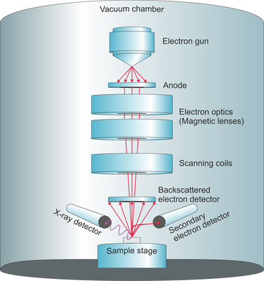
In scanning-electron microscopy (SEM), images are generated by raster-scanning a focused electron beam over a sample and detecting the secondary electrons emitted or the electrons backscattered by the sample. Because electrons can be focused more tightly than light, SEM provides access to spatial resolutions in the nanometer range.

|
In order to increase the mean free path of electrons, the electron optics and sample are placed into a vacuum chamber. Thus, samples have to be vacuum-stable. Depending on the employed detector, SEM provides different image contrasts, which are based on different penetration depths and sample properties.

|
Secondary electron imaging (SEI)
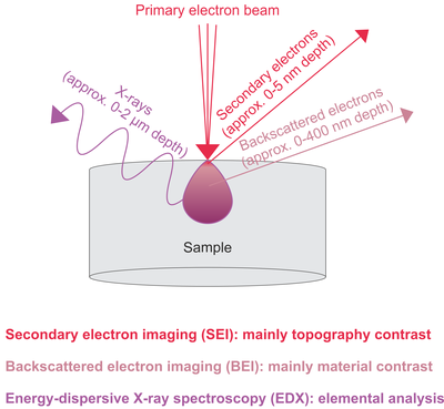
In secondary electron imaging (SEI) the secondary electrons emitted from the atoms of the sample are detected. As a part of the excitation energy is consumed for the extraction of electrons from the electron clouds (work function), with their relatively low kinetic energy secondary electrons can only escape from the top few nanometers of the sample to reach the detector. The image contrast mainly reflects the surface topography of the sample.
Backscattered electron imaging (BEI)
The backscattered primary electrons reaching the detector typically represent the top few 100 nm of a sample. Not primarily influenced by surface corrugation, BEI mainly visualizes the distribution of different chemical elements, which is also referred to as material contrast. High-order-number elements scatter the incoming electrons efficiently and therefore appear bright in BE images.
Energy-dispersive X-ray spectroscopy (EDX)
SEM instruments often also provide X-ray emission spectroscopy with an energy-dispersive spectrometer (EDX). Sample atoms that absorb incoming electrons can emit X-ray spectra containing element-specific emission lines. Typically, X-rays generated within the top 2 µm of a sample can reach the detector. Either single spectra from specific spots or EDX maps representing spatial distributions of chemical elements can be acquired.
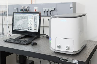
JEOL JCM-6000 Neoscope ESEM-EDX

Our Jeol JCM-6000 Neoscope provides:
- SEM imaging with up to 60000x magnification
- high-vacuum (approx. 10-4 mbar) and low-vacuum modes (around 1 mbar),
- The ESEM (environmental SEM) low-vacuum mode can handle most non-conductive (insulating) samples, which are problematic due to charging effects in high-vacuum mode.
- In low-vacuum mode, the spatial resolution is limited and only BEI and EDX (no SEI) are available.
- EDX spectra acquisition of single spots or averaged over selected sample areas,
- EDX maps based on selected peak intensities representing elemental distributions,
- very easy operation with mouse and touch screen.
Be aware, that our simple table-top instrument cannot compete with high-end SEM systems in terms of spatial resolution, which in our case is more in the sub-micrometer (hundreds of nanometers, depending on the sample) than in the real nanometer range. The benchtop ESEM is not made for imaging in the lower nanometer range (e.g., nanoparticles), its main power is the elemental analysis data that is complementary to the molecular microspectroscopy data provided by Raman microscopy.
We do not have the possibility to coat non-conductive samples with conductive (for example, gold or carbon) layers. Most insulating samples can be imaged in low-vacuum (ESEM) mode, if charging effects occur in normal high-vacuum mode. If you need high spatial resolution or precisely quantitative EDX data, please provide either conductive or specially prepared samples, or look for a specialized SEM lab.
